

The Passivated Emitter Rear Contact (PERC) solar cell architecture demands an
efficient method to form
localized uniform back surface field regions. Hence, the opening of the rear side
thin dielectric layer
without creating many damages to the silicon substrate underneath holds a vital
role. Among the various
methods such as photolithography, chemical etching, diamond scratching, laser
ablation has the
advantage as a fast, accurate, and cost-effective process. However, laser ablation
is a thermal process;
it is essential to choose optimal process parameters such that thermal damage of the
silicon substrate
is minimal without compromising on productivity. This has been achieved using a
synergistic approach
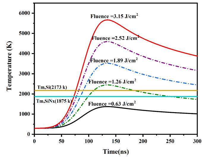
involving computational modelling, experiments, and process optimization (see figure
below). We have
developed a computational model of the laser heating process incorporating a double
layer (passivation
layer coated silicon substrate) to determine a ballpark estimate of the range of
process parameters
based on the temperature profiles as shown in the figure on the left below.
Further, experiments were carried out in the range of process parameters obtained
from the
computational model. Silicon oxynitride dielectric layer of thickness 85 nm was
deposited using plasmaenhanced
chemical vapour deposition system on single side polished silicon wafers. Green 532
nm laser
developed at Sahajanand Laser Technology Ltd., Gujarat, India was used for carrying
out the
experiments. The repetition frequency of 30kHz, speed of 60 mm/sec, the pulse width
of 80 ns and spot
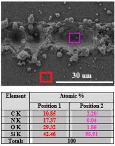
size of 17 μm were used in this study. The effectiveness of laser ablation was
studied using surface
imaging by field emission scanning electron microscope (FESEM) and energy dispersive
spectroscopy
(EDS). The reduction in the elemental percentage of nitrogen and oxygen at position
2 in the figure on
the right below, validates the ablation of the silicon oxynitride layer.


anilkg@ee.iitb.ac.in
dmarla@iitb.ac.in