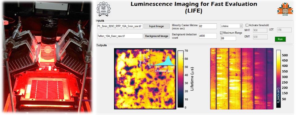
Photoluminescence imaging of silicon using a camera produces a spatial lifetime map of photo-generated carriers in silicon. This enables tracking of changes in the carrier lifetime at different stages of processing and helps optimize the process. Researchers in NCPRE have developed a photo- and electro- luminescence (PL/EL) imaging tool shown below. The tool consists of an LED array excitation source, a probe station for contacting the cell and a camera with suitable filters to cut off the excitation wavelength. Software (LIFE) converts the luminescence intensity to a spatial map of lifetime. This tool facilitated the development of baseline process including economical texturization process, low cost emitter passivation and optimization of metallization etc. This tool has also been used to support the various PV and allied industries in India for Si wafer quality check, process troubleshooting and identification of root cause of device performance degradation.